
The source for all your thin Film needs since 1988.
circuit fabrication
Circuit fabrication is a specialized process at the heart of electronics manufacturing, involving the creation of intricate electronic circuits on various substrates. This meticulous process involves the deposition of thin films as one of the critical steps, followed by photo lithography and various other steps to finally finish a completed circuit. Circuit fabrication is fundamental to the production of electronic devices, such as microchips (used in just about everything these days, like in cell phones, computers, autos and medical equipment) and the whole process can only be accomplished by a handful of very large corporations in the world. However, there are also requirements for small volume circuits, with much larger geometries and which can be addressed by small companies like ours.
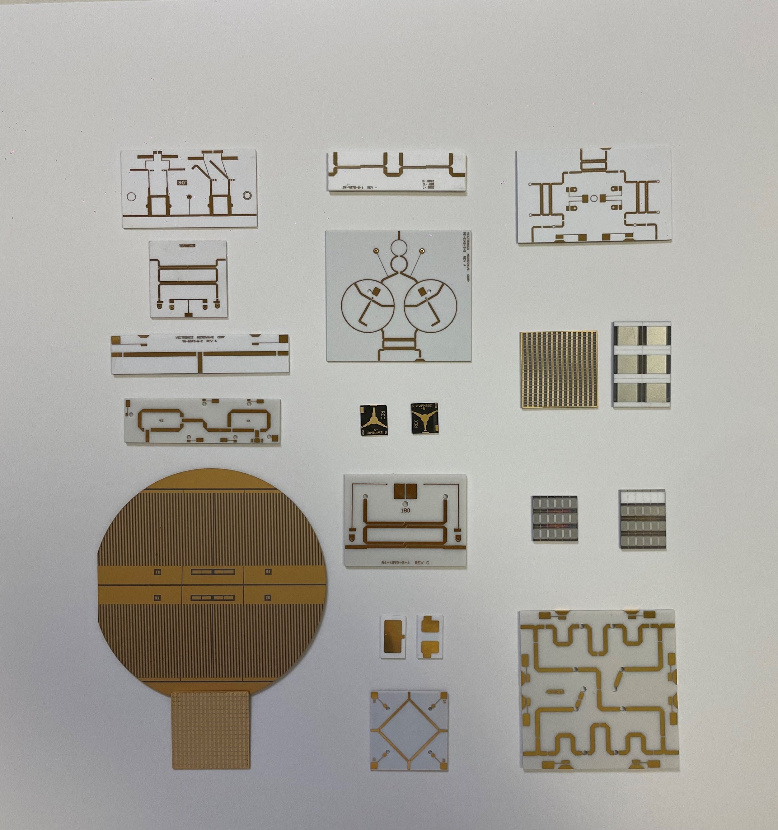
Circuit Fabrication using Photo lithography and Ion Milling
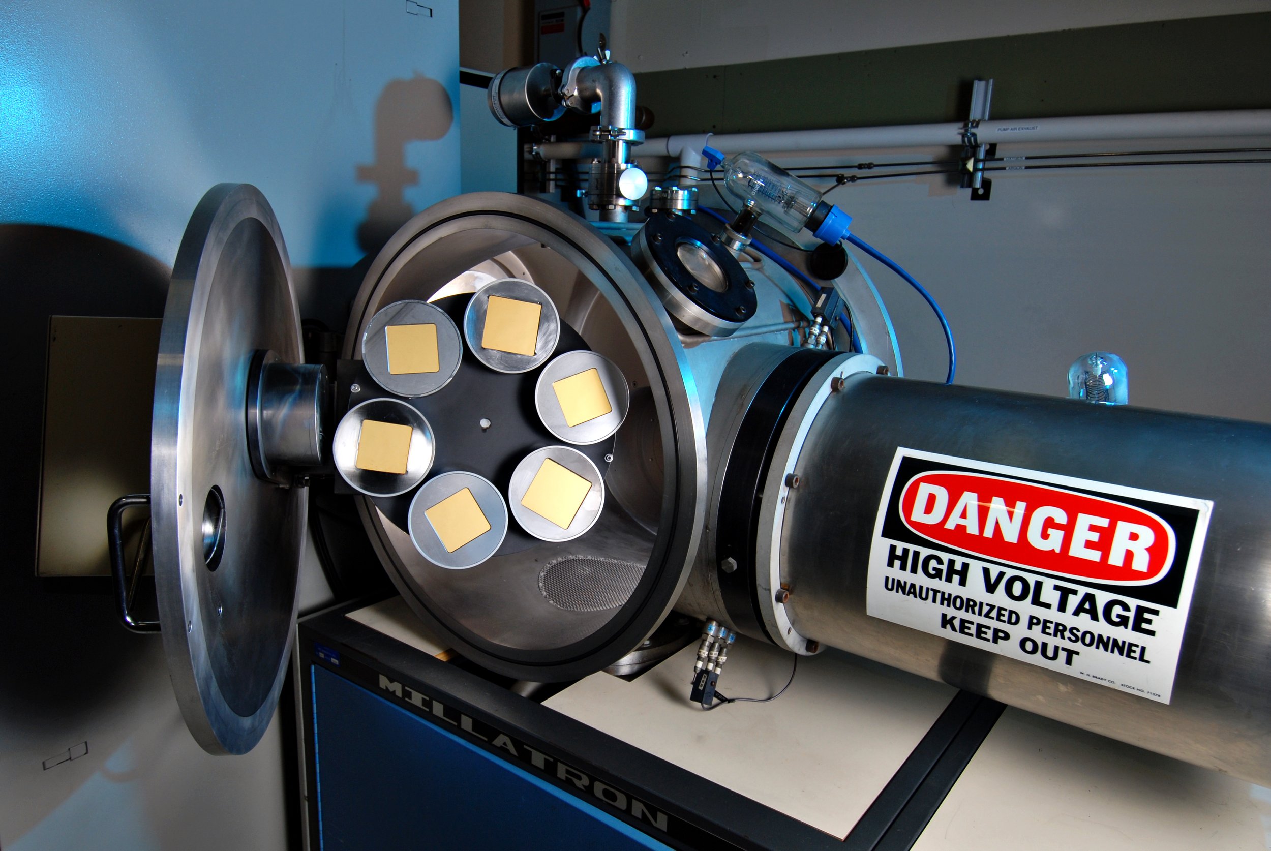
Thin film circuit fabrication and thin film component manufacturing is performed using both wet and dry etching (ion milling and RIE) techniques.
Components are manufactured according to your designs using conductors and resistors. Circuits with through hole vias, front and back metallization can be accommodated. Substrates commonly used include Polished or Lapped Al2O3, BeO, AlN, Si, Ferrites, Diamond, Fused Silica and Titanates.
Please contact us if you require information on other types of materials. We accept all drawings in DXF, DWG or GDS format.
THIN FILM FABRICATION DESIGN RULES:
Minimum line width and gap width, 0.0005”, Tolerance +/- 0.0002”
Metallized or clearance holes-Absolute location +/- 0.002″
Hole taper 10-20% of substrate thickness
Metallized hole minimum 0.005″, capture pad minimum 0.005″
Minimum diameter 1:1 aspect ratio of substrate thickness
Laser cutouts 0.003″ minimum radius
Minimum separation of laser holes is substrate thickness
Metallization pullback from edge 0.002″
Front to back registration +/-0.002″
Edge of via to edge of metallization 0.004” min.
Resistor length and width is 0.002” min. and 0.002” min., respectively
Spacing from via edge to substrate edge 0.01” min. or substrate thickness
Diamond dicing L and W +/-0.001″
TaN-Standard is 50 ohms/sq. Values from 25 to 200 ohms/sq.
TCR is -100 +/-50 ppm/C
Stabilization 425C for 30 minutes, Lower temperature stabilization required for TaN/TiW/Ni/Au to prevent Ni diffusion, 325C for 60 minutes is usual
Layout for passivation is 100% of nominal value, +/- 10%
NiCr-Standard is 50 to 200 ohms/sq.
TCR value is 0 +/- 50 ppm/C
Stabilization is 325C for up to 60 minutes
Layout for laser trimming is 80% of nominal value
Layout for passivation is 100% of nominal value +/- 10%